機能材料暨電子設備事業群
Functional Materials & Electronic Equipment Group
機能材料及電子設備事業群(FMEG,Function Material and Electronic Equipment Group)為公司最初成立的事業部門,前身為機能材料及製品事業群。事業初期以包裝及建材用的塑膠薄膜商品外銷,發展至今產品線橫跨異業領域。包括光學膜產品代理及相關設備銷售、醫藥產品外銷、國內醫療器材、健康食品及建材產品的代理販售事業。
本事業群逐年成長,內外銷實績不斷擴大,異業橫向發展,目標是成為具有國際化綜合商社的機能的事業單位,能夠服務國內外客戶群,與客戶共同創造價值。並同時協助國內企業擴大國際市場商機。
還有任何不了解的地方嗎?
歡迎洽詢本公司
- T886-2-2658-8229
- F886-2-2658-8447
- Esic@skwentex.net
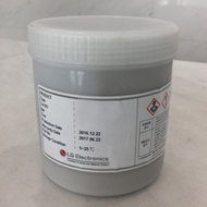
LGE太陽能漿料
代理LGE 太陽能漿料產品,提供高效太陽能電池應用。
【產品線】
提供高效n型雙面、p型傳統矽晶太陽能電池(自2005)、與高效無網結與背接觸表面鈍化太陽能電池高品質量產正銀漿料產品,與客製化與技術整合服務。
【主要特色與效益】
●傳統製程
●Higher efficiency
‧ Excellent electrical Contact to n-Si layer
‧ Suitable for shallow junction emitter ( ≤ 110 Ω/sq )
‧ Low series resistance (Low Rs)
‧ Wide firing window
●Better printability
‧ High resolution : finger widths (≥ 33㎛)
‧ Excellent fine line uniformity
●Properties of paste
Properties | Value |
Viscosity Brook Field HB type Cone & Plate CPE-51 Spindle @ 2.5RPM, 25℃ | 100 ± 20 Pa.s |
Solid contents | 91.0 ± 1.0 % |
Fineness of grind (4th / 50%) | <10㎛ / <7㎛ |
●無網結技術
●Higher efficiency
‧ Excellent electrical Contact to n-Si layer
‧ Suitable for shallow junction emitter ( ≤ 110 Ω/sq )
‧ Low series resistance (Low Rs)
●Better printability
‧ High resolution : finger widths(≥ 25㎛ @ Stencil-mesh)
‧ More Excellent fine line uniformity
‧ Good Aspect ratio
●Properties of paste
Properties | Value |
Viscosity Brook Field HB type Cone & Plate CPE-51 Spindle @ 2.5RPM, 25℃ | 100 ± 20 Pa.s |
Solid contents | 91.0 ± 1.0 % |
Fineness of grind (4th / 50%) | <10㎛ / <7㎛ |
●背接觸表面鈍化技術
●Higher efficiency at PERC
‧ Excellent electrical contact at lower peak firing temperature
‧ Wide firing window & Low firing temperature (30~40℃ lower)
‧ Suitable for shallow junction emitter ( ≤ 110 Ω/sq )
‧ Low series resistance (Low Rs)
●Better printability
‧ High resolution : finger widths (≥ 30㎛)
‧ Excellent fine line uniformity
●Properties of paste
Properties | Value |
Viscosity Brook Field HB type Cone & Plate CPE-51 Spindle @ 2.5RPM, 25℃ | 100 ± 20 Pa.s |
Solid contents | 91.0 ± 1.0 % |
Fineness of grind (4th / 50%) | <10㎛ / <7㎛ |
●n型雙面高效池技術
正面
‧ For N-type wafer with P+ surface
‧ High electronic efficiency at low temperature
‧ High resolution (≥36㎛)
‧ Low series resistance (Low Rs)
‧ Wide process window
‧ Excellent solderability
背面
‧ For N-type wafer with N+ surface
‧ High electronic efficiency at low temperature
‧ Suitable for emitter designs (≤ 60Ω/sq)
‧ Good yield with lower paste consumption rate
‧ Wide process window
‧ Good solderability
還有任何不了解的地方嗎?
歡迎洽詢本公司
- T886-2-2658-8229
- F886-2-2658-8447
- Esic@skwentex.net
